POST Title
Silicon Photonics: Powering Next Era of Computing
- Silicon photonics is becoming a critical enabler of AI and HPC, breaking the limits of electrical interconnects in bandwidth, distance and power efficiency.
- Co-packaged optics (CPO)builds on silicon photonics, with SiPh transceivers as the integration platform and CPO as the packaging architecture that brings optics onto GPUs, CPUs, and switches for higher bandwidth and efficiency.
- Google, NVIDIA, TSMC, AMD, Broadcom and Ayar Labs are all integrating silicon photonics into their core strategies for AI infrastructure.
- TSMC’sCOUPE platform combines advanced logic (N7 and beyond) with mature photonics (65nm SOI), enabling 224 Gb/s interconnects and scalable WDM solutions.
- CPO is an emerging advanced semiconductor packaging (ASP) and is considered the key architecture, bringing optics directly onto GPUs, CPUs, and switches to reduce energy per bit below 5 pJ.
- The industry faces challenges in thermal management, packaging integration, and standardization, but consensus is clear – silicon photonics is not optional for the AI era.
This report summarizes the highlights of the Silicon Photonics Forum at Semicon Taiwan, where this author was among the speakers. In addition to sharing personal insights, the report also examines the unique technological approaches of leading industry players.
1. Introduction to silicon photonics
Silicon photonics integrates optical components — lasers, modulators, waveguides and detectors — into silicon using CMOS-compatible processes, enabling scalable and low-cost manufacturing of optical interconnects. Unlike copper, which is limited in bandwidth, distance and power efficiency, silicon photonics supports energy-efficient optical communication that overcomes these constraints. With AI and HPC workloads driving power demand to hundreds of kilowatts per rack, the technology is already being deployed in AI clusters, hyperscale data centers, and co-packaged optics (CPO). Industry leaders, including Google, NVIDIA, TSMC, AMD, Broadcom and Ayar Labs, are making it a cornerstone of next-generation compute infrastructure.
2. Advantages and necessity of silicon photonics
The necessity of silicon photonics is tied to four converging factors:
- Bandwidth scaling:Electrical I/O is constrained by RC delay, skin effect and crosstalk, while optical interconnects already deliver200–400 Gb/s per lanewith roadmaps beyond1 Tb/s per fiber.
- Energy efficiency:Today’s links consume ~30 pJ/bit; silicon photonics targets<5 pJ/bit, cutting data center power by an order of magnitude.
- Density and distance:Rack GPUs have scaled from32 to 576, but electrical links cannot cover the needed distances. Optical links support both short- and long-reach communication seamlessly.
- manufacturing:Using CMOS nodes (65nm to 7nm) and advanced integration (copper bonding, SOI wafers, nitride waveguides), silicon photonics achieves scalability and lower cost.
Without silicon photonics, AI data centers would hit insurmountable power, thermal and bandwidth walls within the next decade.
3. Counterpoint insights
AI servers are emerging as the main driver of market growth, projected to surpass traditional servers and account for over two-thirds of shipments by mid-decade and more than three-quarters by 2028. This surge is fueled by large language models (LLMs), multimodal AI, and heavy cloud service provider (CSP) investments from Amazon, Google and Microsoft. Counterpoint notes that CSPs are redirecting capital from traditional servers toward AI infrastructure, with the bulk spent on AI servers, accelerators, GPUs and high-speed memory.
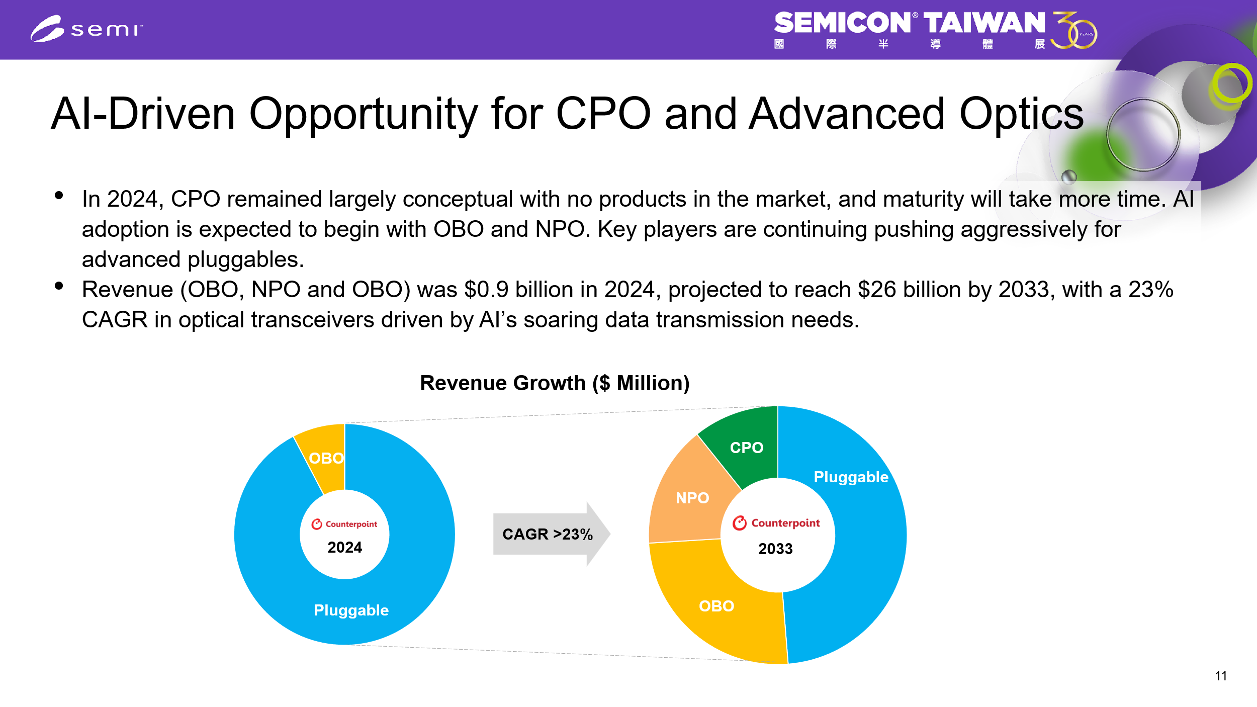
Within this shift, silicon photonics is seen as the backbone of AI data centers, offering faster speeds, lower power, and less heat than electrical links. The market is projected to approach $6 billion by 2030, driven primarily by data centers. Counterpoint also underscores the role of CPO as essential for meeting the bandwidth and performance demands of next-generation AI servers.
NVIDIA announced at GTC 2025 in March that its Spectrum-X will incorporate CPO in the “Photonics” variant, with low-volume production expected to start in the second half of 2026. Broadcom announced on June 3, 2025, that it had begun shipping the Tomahawk 6 switch series, the world's first 102.4 Tbps Ethernet switch chip, which includes native support for CPO technology.
IMAGE
Source: Counterpoint
4. Google’s vision
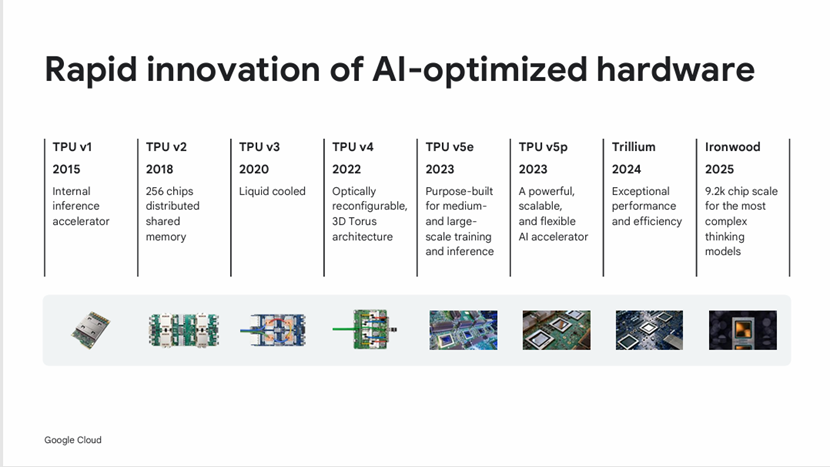
Google sees silicon photonics as critical to its AI infrastructure, scaling alongside the evolution of models likeGemini. To meet rising compute demands, it has built custom hardware such as theTPUv7 IronFord, which delivers 5x the compute and 6x the edge-drain capacity of its predecessor. Its AI supercomputers now exceed 9,000 TPUs, linked by optical technology to provide the high bandwidth and low latency required at scale. Google’s Inter-Chip Interconnect (ICI) supports short-range, high-speed pod communication, while DCI fabrics connect data centers. To ensure reliability, optical circuit switching (OCS) dynamically reroutes traffic during failures. Looking forward, Google is targeting 400 Gbps per lane, an 8x jump in less than a decade, through silicon photonics and CPO, integrating compute and interconnects as its “secret sauce” for AI supercomputing.
IMAGE
5. NVIDIA’s solution
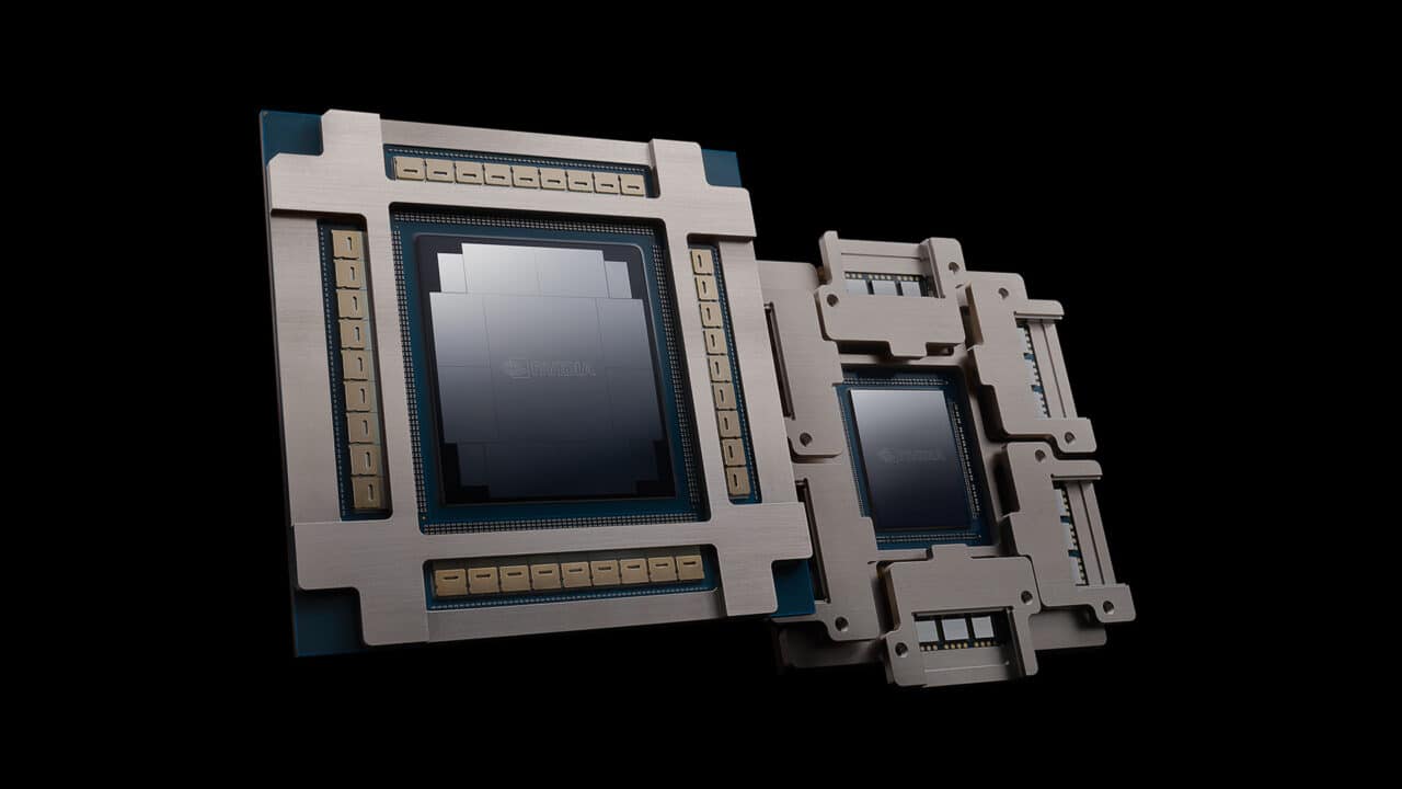
NVIDIA is leading the CPO revolution, positioning it as vital to scaling AI supercomputers. Its data center design spans three layers – Scale-Up (linking ASICs into a single GPU), Scale-Out (connecting hundreds of thousands of GPUs across a data center), and Scale-Across (linking multiple data centers into a mega AI system). With the principle that “the network defines the data center”, NVIDIA sees optical interconnects as essential to moving beyond copper’s limits.
At the core of its scale-out strategy is Spectrum-X Ethernet, a version of Ethernet optimized for AI with RDMA and lossless communication. NVIDIA is integrating CPO into Spectrum-X switches, using micro-ring modulators and advanced packaging via partners like TSMC. A key innovation is the adoption of high-power external laser sources (ELS), front-accessible for replacement, which reduces components and improves resilience. With CPO, NVIDIA can run 3x more GPUs per data center within the same power and cost envelope, achieving 2x bandwidth density, 6x signal energy, and fewer lasers and components overall.
IMAGE
6. TSMC’s process
TSMC is driving mass adoption of silicon photonics through its COmpact Universal Photonic Engine (COUPE), a 3D optical engine that hybrid-bonds an electronic IC (EIC) to a photonic IC (PIC) using copper-to-copper direct bonding to minimize parasitics. The PIC integrates key components such as 200G micro-ring modulators, topped with an oxide layer and a second silicon wafer, with through-dielectric vias providing electrical connections to the EIC.
The platform supports both edge couplers for broadband use and grating couplers for flexibility, wafer-level testing and easier alignment, critical for large-scale optical I/O. TSMC also offers a photonic PDK with standardized building blocks, enabling high-performance PIC design with tight process control.
Focusing on high-volume manufacturing, TSMC uses mature 65-mm SOI wafers and advanced tools to keep dimensional variation within 2 mm across wafers. It has already demonstrated 224 Gbps per lane optical interconnects and is exploring materials beyond silicon for higher speeds. COUPE further reduces costs by allowing passive testing at multiple wafer stages.
7. AMD’s vision
AMD sees Moore’s Law slowing even as AI demand accelerates, pushing the need for CPO to scale its next-generation chips. Its new MI350/355 AI processor, built with 3D stacking, memory-on-core bonding and 180B transistors, faces challenges in heat dissipation and mechanical stress due to its size and power.
To overcome bandwidth and scaling limits, AMD is developing end-to-end CPO integration flows, treating optics as a core part of the manufacturing process. A major hurdle is achieving high-volume connector alignment, where edge couplers offer higher bandwidth but are harder to manage at wafer scale, while grating couplers are easier but bandwidth-limited. AMD is also exploring laser integration, balancing between on-chip lasers for compactness and external lasers for reliability.
As both a photonic foundry and ODM customer, AMD stresses supply-chain collaboration to ensure manufacturable, scalable solutions for the massive AI workload ahead.
8. Broadcom’s solution
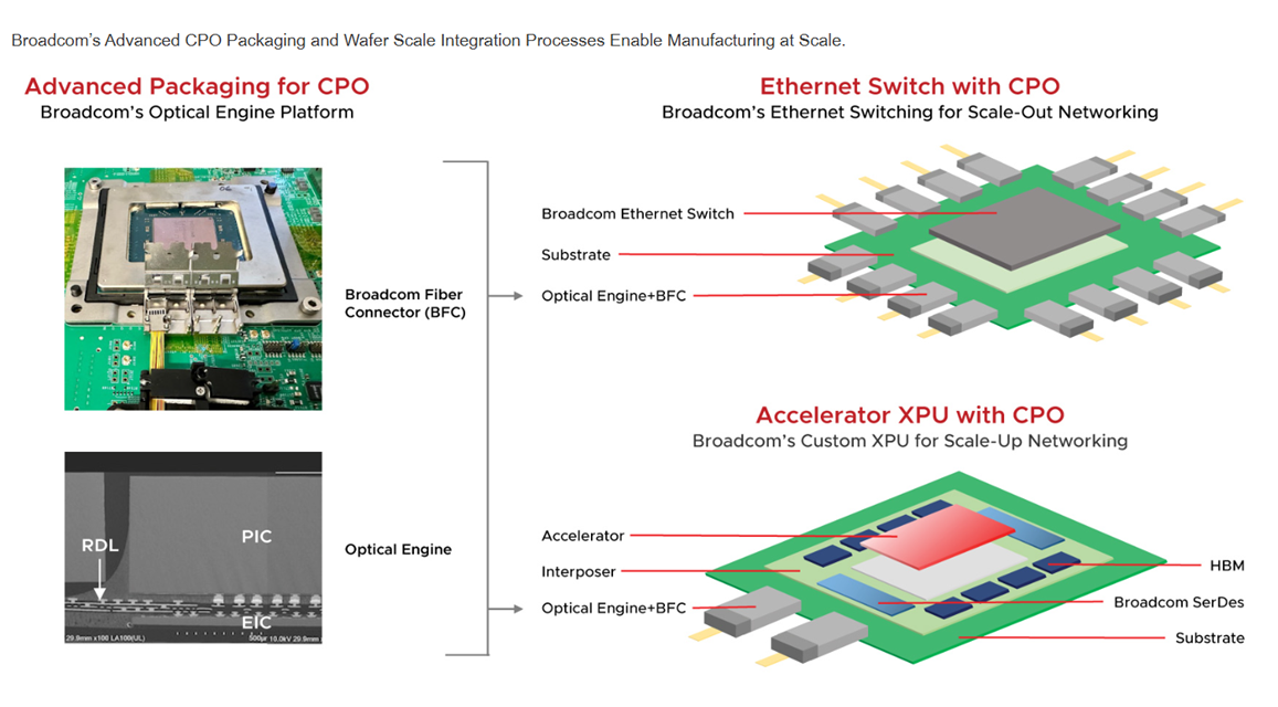
Broadcomsees silicon photonics as a cost-effective, power-efficient enabler of large AI networks, focusing on two technologies – VCSEL NPO and CPO. VCSEL NPO leverages mature, low-power VCSEL devices already proven in high-volume manufacturing, sustaining up to 6.4 Tbps and scaling toward 200 Gbps per channel. For higher density and longer reach, Broadcom is advancing CPO on silicon photonics, targeting ~6 pJ/bit and validating reliability through stress tests, including exposure to Arizona dust.
The company emphasizes that widespread adoption requires progress in cost, reliability and escape bandwidth, as well as interoperability across vendors. Broadcom is collaborating with customers and industry peers to ensure CPO systems can be deployed reliably at scale without component failures.
IMAGE
9. Ayar Labs’ solution
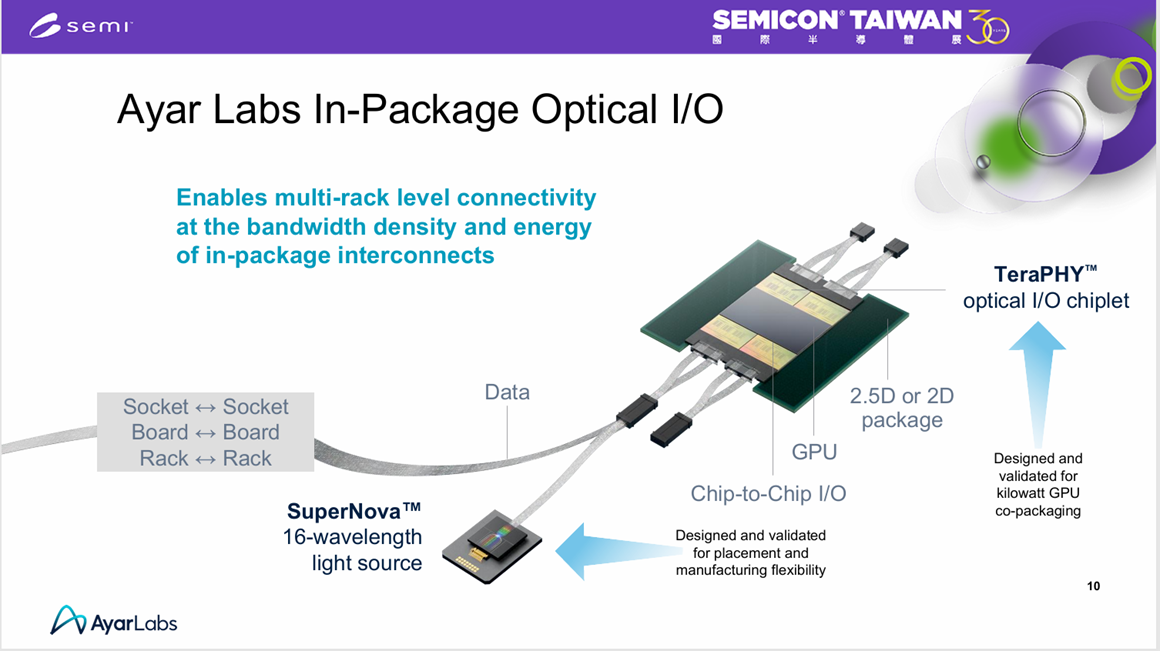
Ayar Labs is pioneering optical I/O chiplets, compact devices that convert electrical signals to optical signals and are co-packaged with high-performance SoCs. Its Supernova external light source (ELS) platform uses single-mode optics to overcome the bandwidth-distance tradeoff, working seamlessly from sub-meter rack links to kilometer-scale clusters.
The company demonstrated the world’s first UCIe optical I/O chiplet, a retimer with optical macros delivering 8 Tbps per chiplet, enabling multi-rack fabrics that scale to thousands of GPUs while holding rack-level power constant.
Extensive reliability testing confirms thermal stability under AI accelerator workloads, and simulations show 5-10x better performance and TCO versus electrical interconnects. To scale adoption, Ayar Labs partners with foundries, OSATs and material suppliers, building a robust ecosystem for optical I/O.
IMAGE
Source: AyarLabs
10. Conclusion
AI demand is pushing traditional computing to its limits, and silicon photonics offers the path forward. From Google’s end-to-end infrastructure to NVIDIA’s CPO switches and TSMC’s manufacturing platforms, the industry is uniting around optical interconnects to overcome bottlenecks in bandwidth, power and heat. The move from discrete transceivers to CPO marks a fundamental shift in AI data center design. Companies such as AMD, Broadcom and Ayar Labs are driving innovations in chip design, packaging, materials and testing to enable high-volume production. Once seen as futuristic, silicon photonics has become the backbone of the AI era.
IMAGE
Receive our insightful weekly newsletter and stay ahead of the competition.
Author
Peter Richardson

Peter has 27 years experience in the mobile industry with extensive experience in market analysis and corporate development. Most recently Peter was Global Head of Market and Competitive Intelligence at Nokia. Here he headed a team responsible for analyzing and quantifying the industry. Prior to Nokia, Peter was an equity analyst at SoundView Technology Group. And before that he was VP and Chief Analyst of mobile and wireless research at Gartner. Peter’s early years in the industry were spent with NEC and Panasonic.